Conduction Band and Valence Band Showing Energy Levels, Electron Transition, and Semiconductor Concept
In the world of solid-state physics and modern electronics, the concepts of the valence band and conduction band form the foundation of how materials behave electrically. These two energy levels describe the arrangement and behavior of electrons inside solids, determining whether a material acts as a conductor, semiconductor, or insulator. A vector illustration showing the conduction and valence bands highlights not only the vertical energy separation between these regions but also the movement of electrons across the band gap, the defining feature that controls current flow in semiconductors. Although the illustration itself appears simple — with stacked horizontal bands separated by a visual gap — the story behind it explains how everyday technologies like smartphones, solar cells, LEDs, processors, and sensors function.
The valence band is the range of electron energy levels where electrons are normally bound to atoms, contributing to chemical bonding rather than electrical conduction. In a semiconductor or insulator, electrons in the valence band are tightly held in place and cannot move freely. They participate in maintaining the crystal structure of the material by forming stable bonds between atoms. Because electrical current depends on mobile charge carriers, a material with only filled valence band electrons cannot conduct electricity. In an illustration, the valence band is often shown at the lower part of the diagram, densely filled with electrons to represent stability and limited mobility.
The conduction band, positioned above the valence band in energy diagrams, contains electron states that are not involved in bonding and are available for electrical transport. When electrons occupy this band, they gain the freedom to move throughout the crystal lattice, allowing electrical current to flow. In a visual representation, the conduction band is drawn above the valence band with more open energy slots to symbolize that electrons can move and accelerate when an electric field is applied. For conduction to occur, electrons must transition from the valence band to the conduction band — a movement that requires energy because the conduction band lies at a higher energy level.
The separation between these two bands is called the band gap. This gap determines how easy or difficult it is for electrons to jump from the valence band into the conduction band. In conductors (such as metals), the conduction and valence bands overlap, meaning electrons already have access to conduction states and flow freely without an external energy boost. In insulators, the band gap is extremely large, preventing meaningful conduction because ordinary thermal or electrical energy cannot lift electrons into the conduction band. Semiconductors, however, lie in the middle — with a moderate band gap that electrons can cross if provided with the right amount of energy. This is what makes semiconductors uniquely useful: they can alternate between insulating and conducting states depending on energy input.
In a semiconductor material such as silicon, electron transition from the valence band to the conduction band can occur through several mechanisms. Thermal energy at room temperature provides enough excitation for a small portion of electrons to cross the band gap. As electrons move into the conduction band, they leave behind empty positions in the valence band called holes, which act as positive charge carriers. Thus, electrical conduction in semiconductors involves both motion of electrons in the conduction band and movement of holes in the valence band. A vector illustration often marks this by showing an electron arrow moving upward across the band gap and a corresponding hole left behind below.
Electrons can also be promoted across the band gap through light absorption, forming the basis of solar cell technology. When photons with sufficient energy strike a semiconductor, they transfer energy to electrons, enabling them to move into the conduction band. Conversely, when electrons fall back from the conduction band to the valence band, they release energy in the form of light — a mechanism used in LEDs and semiconductor lasers. These transitions illustrate the dual role of the band gap: it is a barrier to conduction under normal conditions but a gateway to energy conversion when stimulated.
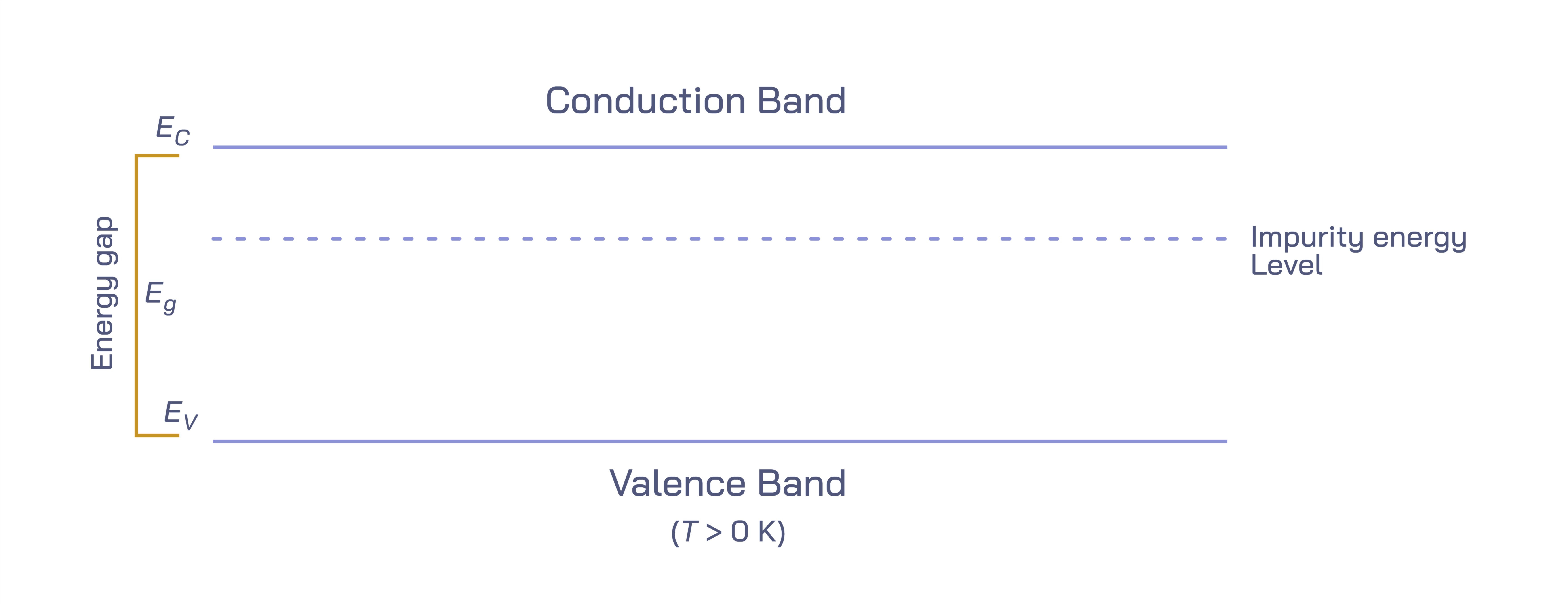
Another essential semiconductor concept shown in band diagrams is doping, which intentionally adds impurities to modify conductivity. Adding phosphorus atoms to silicon introduces extra loosely bound electrons, creating an n-type semiconductor where electrons dominate conduction. Adding boron creates p-type material, supplying more holes for conduction. In energy diagrams, doping appears as added energy levels close to the conduction or valence band, reducing the energy required for transitions and strengthening conductivity. When p- and n-type regions are combined, the band alignment creates a p-n junction, the core of diodes, transistors, rectifiers, and solar cells. Even without mathematical detail, a visual depiction of band bending at the junction immediately communicates why current flows in one direction and not the other.
Temperature also plays a role in electron behavior within bands. As temperature increases, more electrons gain enough thermal energy to cross the band gap into the conduction band, increasing conductivity. The reverse is also true: cooling reduces available energy and decreases conductivity. Because conductivity varies predictably with temperature, semiconductors operate as sensitive sensors in electronic devices. Their electrical response to heat forms the foundation of temperature detectors, automatic controls, and thermal management systems.
Ultimately, a band diagram showing conduction band, valence band, and band gap is much more than a neat classification of energy levels — it is a blueprint for every modern electronic innovation. It explains how a semiconductor chip can amplify signals, how a diode can allow current to move directionally, how a solar panel converts sunlight into electricity, how a transistor switches billions of times per second inside a processor, and how modern lighting uses electrical energy to generate photons.
In a full vector illustration, the concepts synchronize visually:
• A lower valence band filled with electrons.
• An upper conduction band with room for electrons to move freely.
• A band gap separating the two, symbolizing the energy needed for electron transition.
• Upward arrows showing excitation and downward arrows showing energy release.
• Optional added levels showing doping effects and modified conductivity.
Even if the drawing includes no equations and no mathematical symbols, it communicates a powerful message: electrical conduction is governed not by the physical arrangement of atoms alone but by the energy landscape that electrons inhabit. The conduction and valence band model distills this complexity into a clear, intuitive structure where the flow of electrons becomes both a microscopic event and the engine behind global electronics.
Through the lens of this model, semiconductors become more than just materials — they become controllable systems that make computing, communication, power conversion, sensing, and lighting possible. The band diagram thus stands as the central graphic representation of electronic physics, capturing in a simple visual the key interplay between energy levels, electron transitions, and technological possibility.