Difference Between N-Type and P-Type Semiconductors: A Detailed Description
Understanding the Role of Doping in Transforming Semiconductors
Pure silicon has limited conductivity because its electrons are tightly bound within covalent bonds. To enhance its electrical behavior, scientists introduce controlled impurities into the crystal lattice—a process known as doping. Depending on the type of impurity added, silicon becomes either N-type or P-type, each with unique charge carriers and conduction properties. These doped materials form the basis of modern electronics, enabling the functioning of diodes, transistors, solar cells, and integrated circuits. This transformation from intrinsic to extrinsic semiconductor behavior allows precise control over how current flows through a material.
N-Type Semiconductors: Dominance of Free Electrons
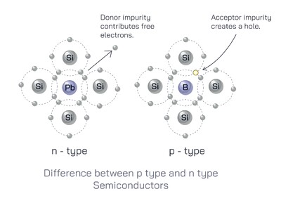
N-type semiconductors are created by adding pentavalent impurities such as phosphorus, arsenic, or antimony to silicon. These atoms carry five valence electrons—one more than silicon requires to complete four covalent bonds. When integrated into the lattice, four electrons form stable bonds with surrounding silicon atoms, leaving one loosely bound electron free to move. This additional free electron significantly increases conductivity.
Because electrons vastly outnumber holes in N-type materials, electrons become the majority charge carriers. Holes exist only in trace quantities and act as minority carriers. The donor impurities contribute these electrons and introduce energy levels just below the conduction band, making it easier for electrons to transition and support current flow.
How N-Type Materials Conduct Electricity
When an electric field is applied, the abundant free electrons drift toward the positive terminal, creating current. Their mobility and ease of excitation make N-type materials efficient conductors. Although electrons dominate movement, overall electrical neutrality is maintained because donor atoms carry a balanced positive charge that offsets the freed electrons.
P-Type Semiconductors: Dominance of Holes as Charge Carriers
P-type semiconductors form when trivalent impurities—such as boron, aluminum, or gallium—are introduced into the silicon lattice. These atoms have only three valence electrons and form three complete covalent bonds, leaving one incomplete bond known as a hole. A hole behaves as a positive charge because it represents the absence of an electron.
In P-type material, holes outnumber free electrons and act as the majority carriers. When an electron from a neighboring bond moves to fill a hole, the hole effectively shifts in the opposite direction. This movement of holes is equivalent to current flow. Acceptor impurities introduce energy levels just above the valence band, allowing electrons to jump upward and create mobile holes.
How P-Type Materials Conduct Electricity
Electrical conduction occurs when electrons repeatedly move to fill existing holes, making the holes appear to drift toward the negative terminal. Although holes function as positive charge carriers, the material remains electrically neutral because the acceptor atoms compensate for the missing electrons.
Major Difference: Majority Carriers and Type of Impurity
The essential distinction between N-type and P-type semiconductors lies in their charge carriers:
N-Type → Majority carriers are electrons (negative charge).
Impurity = Donor (adds electrons).
P-Type → Majority carriers are holes (positive charge).
Impurity = Acceptor (creates holes).
This difference influences conductivity, device behavior, and how each material responds inside electronic components.
Formation of the PN Junction: How N-Type and P-Type Work Together
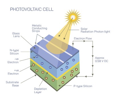
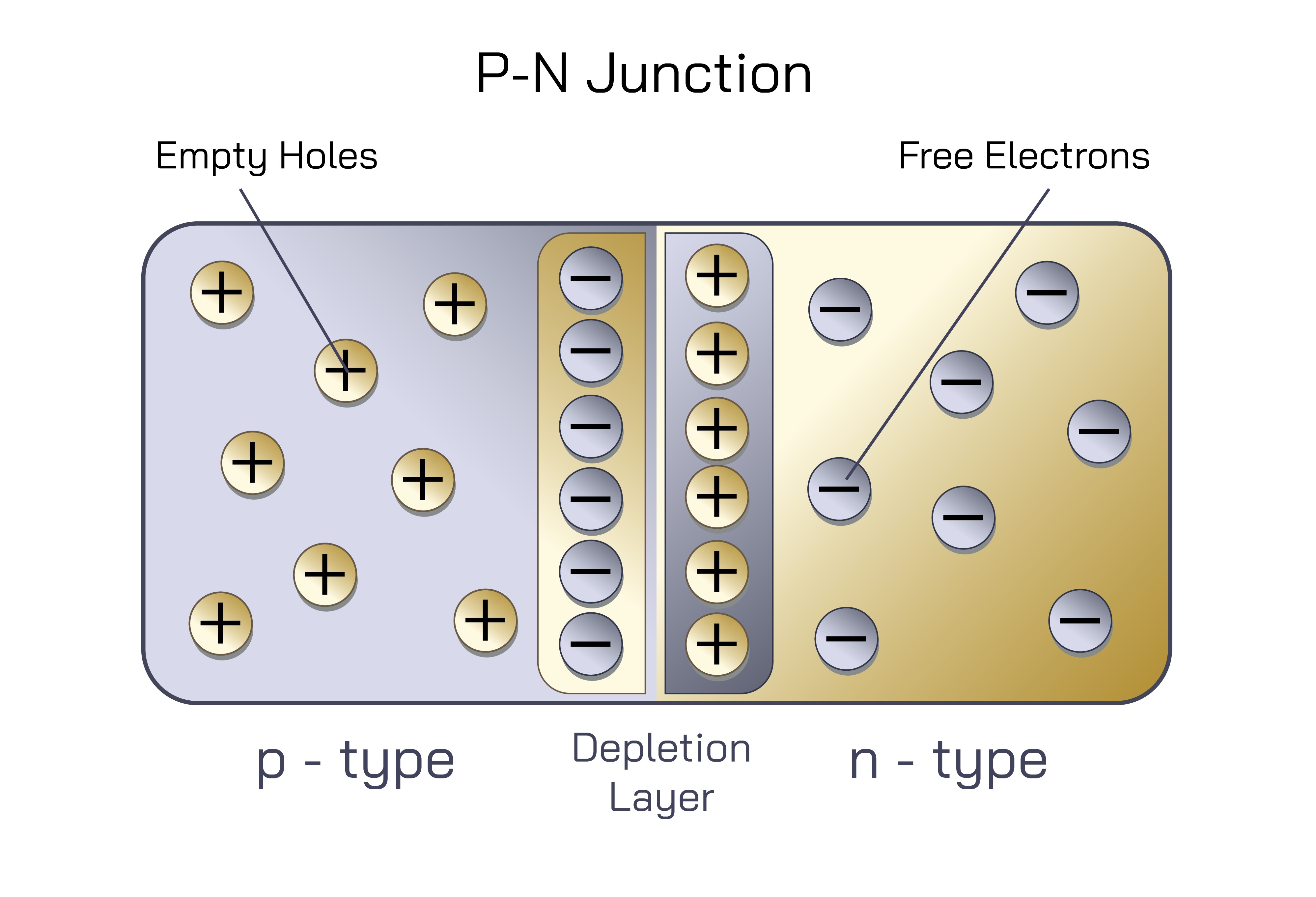
When N-type and P-type materials are brought together, a PN junction forms—one of the most important structures in electronics. At the boundary, electrons from the N-region diffuse into the P-region and recombine with holes. Similarly, holes migrate into the N-region and recombine with electrons. This movement depletes both regions of free carriers in a thin boundary region called the depletion layer.
This depletion region develops a built-in electric field that prevents further uncontrolled carrier movement and allows the junction to behave like a diode. The PN junction permits current to flow in one direction but blocks it in the opposite direction. This one-way conduction principle forms the foundation of diodes, transistors, rectifiers, solar cells, and countless integrated devices.
Electrical Behavior Resulting from PN Junction Formation
Forward Bias: Applying positive voltage to the P-side reduces the depletion region and allows current to flow.
Reverse Bias: Applying reversed voltage widens the depletion region and blocks current, except for a tiny leakage.
This switch-like behavior is why semiconductor junctions revolutionized electronics.
Why Understanding N-Type and P-Type Semiconductors Matters
Knowledge of semiconductor types helps explain the inner workings of modern technology—from smartphones to solar panels. The distinction between electron-rich N-type and hole-rich P-type materials enables precise control of current, amplification, switching, and energy conversion. These complementary materials form the heart of microelectronics, making their understanding essential for physics, engineering, and technological innovation.
Together, N-type and P-type semiconductors allow devices to manipulate electrical signals with extraordinary efficiency, laying the foundation for the digital world.