Conduction Band vs Valence Band Showing Electron Energy Levels, Band Gap, and Semiconductor Concept
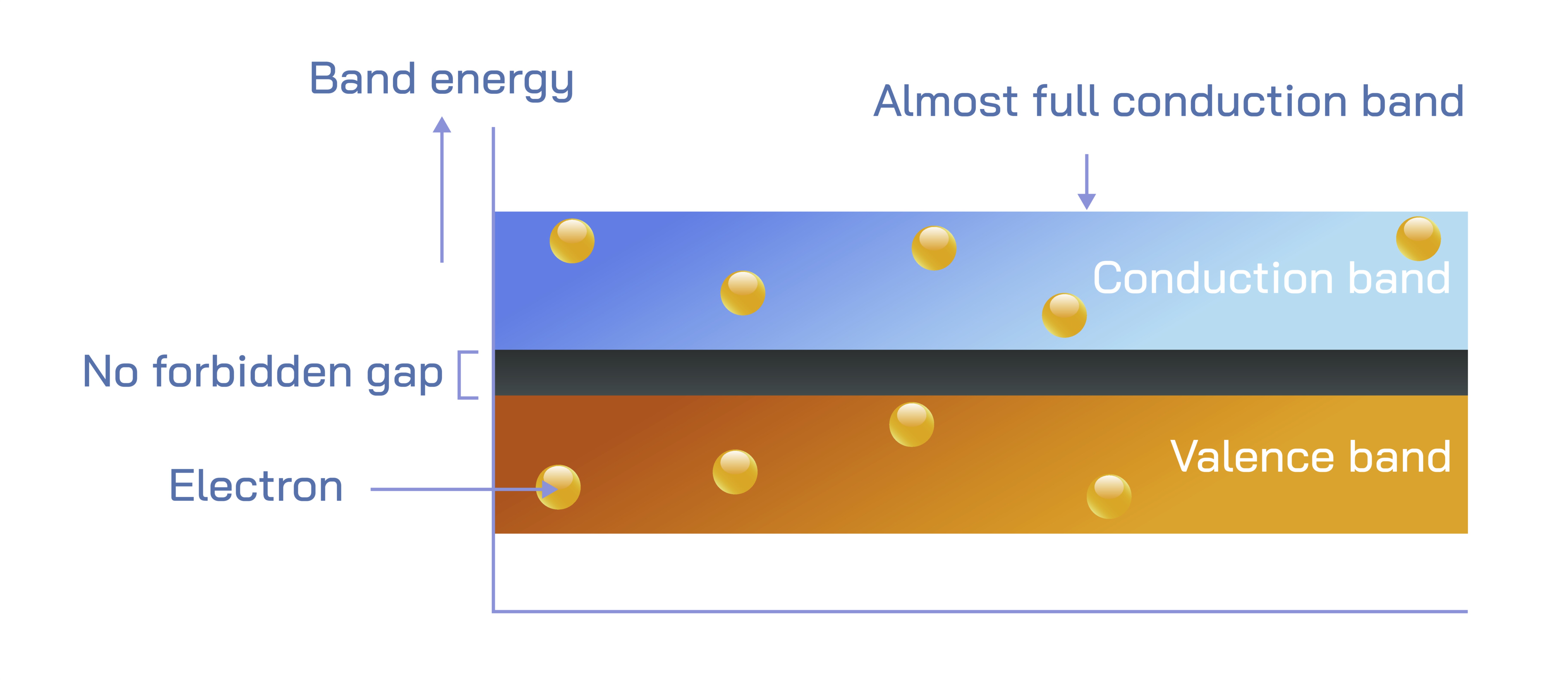
In solid-state physics and materials science, the concepts of conduction band and valence band are fundamental for understanding the electrical properties of materials, particularly semiconductors. A vector illustration comparing the conduction band and valence band usually depicts two parallel energy levels separated by a band gap, along with electrons occupying the valence band and empty or partially filled states in the conduction band. This visual representation makes it clear how electrons gain or lose energy to move between bands, which in turn dictates whether a material behaves as a conductor, insulator, or semiconductor. While the diagram appears simple, it captures the essence of electron mobility, energy transitions, and the microscopic basis of modern electronics, from diodes to transistors to solar cells.
The valence band represents the highest range of energy levels in a material that are normally filled with electrons under equilibrium conditions. Electrons in the valence band are bound to atoms and participate in forming chemical bonds. In vector illustrations, this band is typically drawn below the conduction band, filled with electron symbols to indicate occupancy. The valence electrons determine the chemical behavior of the atom and the solid’s ability to bond with neighboring atoms. For conductors, the valence band overlaps with the conduction band, allowing electrons to move freely. In semiconductors and insulators, the valence band is fully filled at absolute zero, meaning that under normal conditions electrons cannot freely contribute to electrical conduction until they gain sufficient energy to transition into the conduction band.
Above the valence band lies the conduction band, where electrons are free to move throughout the crystal lattice. In illustrations, the conduction band is often shown as partially empty, with room for electrons to enter when excited by thermal energy, light, or an electric field. Electrons in this band are delocalized and act as charge carriers, enabling the flow of electric current. The energy required for electrons to reach the conduction band depends on the material’s band gap, the energy difference between the top of the valence band and the bottom of the conduction band. In semiconductors, this band gap is small enough that external energy — such as heat or photon absorption — can promote electrons into the conduction band, making electrical conduction possible under controlled conditions.
The band gap is one of the most critical parameters illustrated in a conduction vs valence band diagram. It defines the energy threshold that electrons must overcome to transition from being bound in the valence band to being free in the conduction band. Materials with a large band gap, such as diamond, are insulators because thermal energy at room temperature is insufficient to excite electrons across the gap. Materials with a very small or zero band gap, such as metals, allow electrons to flow freely and conduct electricity efficiently. Semiconductors occupy the intermediate space: their band gap is small enough that controlled excitation enables conduction while also allowing precise manipulation of their electronic properties using doping or external stimuli.
Vector illustrations often include electron transitions from the valence band to the conduction band, represented by arrows pointing upward across the band gap. These transitions show how energy input, whether thermal, optical, or electrical, promotes electrons into conduction states. The resulting electron-hole pairs are central to semiconductor operation: when an electron leaves the valence band, it creates a “hole” that can move in the opposite direction, effectively acting as a positive charge carrier. Both electrons in the conduction band and holes in the valence band contribute to electrical current, providing the foundational principle behind diodes, transistors, photovoltaic cells, and other semiconductor devices.
Temperature, doping, and external fields further influence the occupation of the bands. In intrinsic semiconductors at absolute zero, the valence band is completely full and the conduction band completely empty, preventing conduction. As temperature increases, some electrons gain enough thermal energy to cross the band gap, leaving behind holes and generating intrinsic conductivity. Doping introduces impurity levels within the band gap, either donating extra electrons (n-type) or creating holes (p-type), effectively reducing the energy barrier for conduction. Vector diagrams may include these donor or acceptor levels within the band gap to illustrate how engineered materials manipulate electron populations for electronic applications.
The physical significance of the conduction and valence bands extends beyond abstract energy levels. They explain why silicon and germanium can serve as the backbone of modern electronics. When a voltage is applied, conduction band electrons respond to the field, moving through the lattice and enabling current. The number of electrons in the conduction band directly controls conductivity, while the valence band provides the reservoir from which these electrons are excited. Optical phenomena such as absorption, emission, and photoconduction also depend on electron transitions across the band gap, linking the conduction and valence bands to technologies like LEDs, lasers, and solar panels.
A complete vector illustration of conduction vs valence bands typically includes:
Valence band: fully occupied by electrons, positioned below the conduction band
Conduction band: partially empty, allowing electron mobility
Band gap (Eg): energy separation between valence and conduction bands
Electron transitions: arrows showing electrons excited from valence to conduction band
Holes: vacancies left in the valence band acting as positive charge carriers
Optional impurity/doping levels within the band gap to illustrate n-type and p-type semiconductors
By visualizing these energy levels, the diagram conveys how materials control the movement of charge at a microscopic level, forming the foundation of all modern electronics. Electrons jumping across the band gap, holes traveling in the opposite direction, and the ability to manipulate these populations through external energy are what make semiconductors versatile, tunable, and indispensable. A conduction vs valence band illustration is therefore not merely an abstract diagram — it is a blueprint for understanding how energy, matter, and electricity intersect in solid materials to power the devices that define contemporary life.