Difference Between N-Type and P-Type Semiconductors: A Detailed Description
Understanding Why Semiconductors Need Doping
Semiconductors such as silicon naturally have limited conductivity, but their electrical behavior becomes highly controllable when small amounts of impurity atoms are introduced into their crystal lattice. This process, known as doping, transforms pure semiconductors into N-type or P-type materials depending on the kind of impurity added. These doped semiconductors serve as the building blocks of diodes, transistors, solar cells, and nearly every modern electronic device. The reason doping is so powerful lies in its ability to change the balance of charges in the material, creating new pathways for electric current to flow. To appreciate the distinction between N-type and P-type semiconductors, it is important to examine how impurities interact with the silicon lattice and influence the presence of free electrons or holes.
N-Type Semiconductors: Dominance of Free Electrons
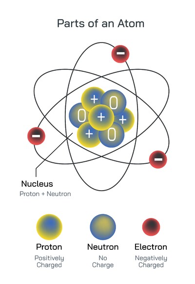
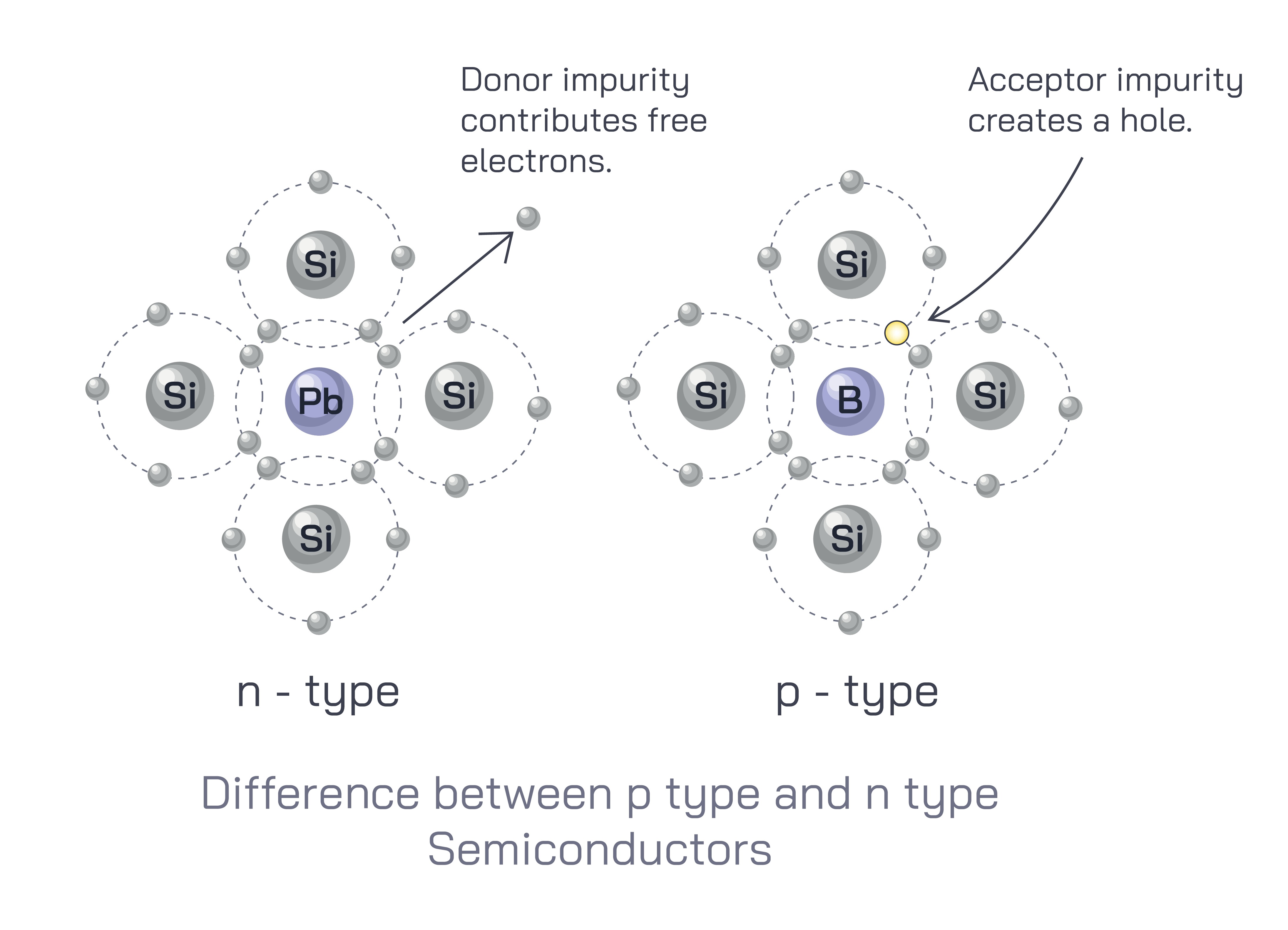
N-type semiconductors are created when a tetravalent semiconductor such as silicon is doped with a pentavalent impurity, typically phosphorus, arsenic, or antimony. These atoms contain five valence electrons—one more than silicon. When incorporated into the lattice, four of the impurity’s electrons bond with neighboring silicon atoms, while the fifth electron remains loosely attached. This extra electron becomes a free electron that can move easily throughout the lattice, greatly increasing electrical conductivity. Because free electrons outnumber holes in N-type materials, electrons become the majority charge carriers, while holes serve only a minor role in conduction. The impurity atoms that donate extra electrons are known as donor impurities because they contribute charge carriers without significantly disrupting the crystal structure.
How N-Type Semiconductors Conduct Electricity
The abundance of free electrons allows N-type semiconductors to conduct electricity primarily through electron flow. When an electric field is applied, these electrons move toward the positive terminal, enabling a steady current. The donor impurities also introduce energy levels just below the conduction band, making it easier for electrons to jump into the conduction band and move freely. This shift in the material’s electronic structure contributes to lower resistance and improved conductivity compared to pure silicon. Despite the increased electron population, the crystal lattice remains electrically neutral because the added impurity atoms balance the excess charge internally.
P-Type Semiconductors: Dominance of Holes
P-type semiconductors arise when silicon is doped with a trivalent impurity such as boron, aluminum, or gallium. These atoms have only three valence electrons—one fewer than silicon. When these impurities are inserted into the lattice, they form three complete bonds with neighboring silicon atoms, leaving one bond incomplete. This creates a vacancy known as a hole, which acts as a positive charge carrier. Holes are not physical particles but represent the absence of an electron; however, they move through the lattice as neighboring electrons shift to fill the empty space. Because holes outnumber electrons, holes become the majority charge carriers while electrons play a secondary role. Impurities that create holes are called acceptor impurities because they effectively accept electrons from nearby atoms.
How P-Type Semiconductors Conduct Electricity
Electrical conduction in P-type materials occurs when electrons move to fill holes, causing the holes to migrate through the lattice toward the negative terminal. The acceptor impurities introduce an energy level just above the valence band, enabling electrons to jump into these empty states and generate mobile holes. This mechanism creates a type of conduction that appears opposite to electron movement but produces the same result: an electric current. Like N-type semiconductors, P-type materials remain electrically neutral as the charge imbalance is internally compensated by the impurity atoms.
Fundamental Difference: Majority Charge Carriers
The key distinction between N-type and P-type materials is the identity of the majority charge carrier. In N-type semiconductors, electrons dominate conduction; in P-type semiconductors, holes take the lead role. This difference influences how each material responds to electric fields, how current flows through them, and how they behave when combined into PN junctions, which are central to electronic components. The complementary nature of electron-rich N-type and hole-rich P-type semiconductors allows engineers to design devices that control current direction, amplify signals, convert sunlight into electricity, and perform countless digital operations.
How These Semiconductors Work Together in Devices
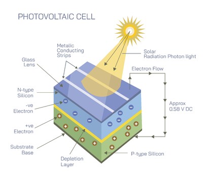
When N-type and P-type materials are joined, electrons from the N-region diffuse into the P-region while holes from the P-region diffuse into the N-region. This movement creates a depletion region where charge carriers cannot move freely. The resulting junction behaves as a diode, allowing current to flow easily in one direction while blocking it in the other. This principle forms the basis for rectifiers, LEDs, transistors, and logic circuits. In solar cells, the junction promotes charge separation after light absorption, enabling electricity generation. The complementary behavior of both types makes modern electronics possible.
Why Doping Level and Impurity Choice Matter
The concentration and type of impurity used in doping directly influence conductivity and device performance. Too much doping may reduce mobility, while too little reduces conductivity. Pentavalent and trivalent impurities are carefully chosen for their compatibility with silicon and the stability they offer within the lattice. These impurities must bond precisely with surrounding atoms without disrupting the material’s structural integrity. As semiconductor technology advances, doping techniques continue to evolve to support smaller, faster, and more efficient electronic components.
The Importance of Understanding N-Type and P-Type Semiconductors
Mastering the difference between N-type and P-type semiconductors is essential for understanding how modern electronics operate. These materials form the basis of digital circuits, microprocessors, sensors, solar cells, and communication devices. By altering the balance between electrons and holes, engineers create versatile and highly controllable materials that power the digital world. Recognizing how impurities influence electrical behavior provides deeper insight into the foundations of semiconductor science and its role in shaping technology.